9DBL0255NLGI8
- Description
- PCIe Gen1 to 5 Clock Fanout Buffer with LOS 2-OUT 16-Pin VFQFPN T/R
- PLL
- Yes
- Max Junction Temperature (Tj)
- 150°C
- Datasheet
Quantity
7,500 AvailableLet us do the sourcing. Even if it's not available now, our team can track it down and tailor a solution just for you.
- PCIe Gen1 through Gen5 clock fanout buffer
- 2 differential outputs
- Loss-of-signal (LOS) detection
- Integrated PLL
- 3.135 V to 3.465 V supply, up to 200 MHz
- 16-pin VFQFN package, -40 C to 85 C
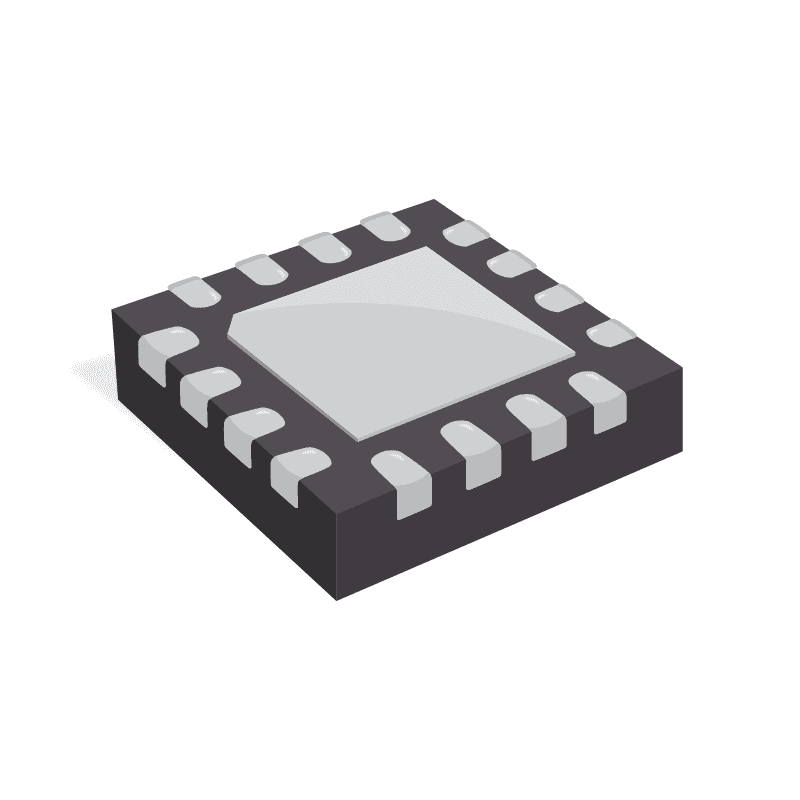
The Renesas 9DBL0255NLGI8 is a two-output PCI Express clock fanout buffer that supports PCIe generations 1 through 5 and includes loss-of-signal (LOS) detection. It operates from a 3.3 V supply (3.135 V to 3.465 V) at frequencies up to 200 MHz and integrates a PLL. The device is supplied in a 16-pin VFQFN package.
This clock buffer is used to distribute low-jitter reference clocks to PCI Express endpoints and switches on server, storage, and networking motherboards and add-in cards. Fanning one reference to multiple outputs preserves signal integrity across PCIe Gen1 to Gen5 links, and LOS detection helps the system flag a missing source clock. It suits datacenter and high-speed digital designs that need reliable PCIe clocking.
Fusion’s in-house quality hubs and Prosemi testing facility are fully certified to meet critical industry standards for electronic component inspection and testing.
Quantity
7,500 AvailableLet us do the sourcing. Even if it's not available now, our team can track it down and tailor a solution just for you.